- U29 pin 5 to P4 pin 12
- U29 pin 6 to P4 pin 13
- U29 pin 13 to pad marked AN3 (near U11)
- U3 pin 14 to P4 pin 11
The premise is simple. The Kantronics KPC-9612+MX TNC is capable of monitoring two analog values (such as battery voltage, or temperature) and transmit these values via an APRS telemetry packet. On a recent repeater site install, we needed to monitor additional values (several battery banks), so I started studying the TNC schematics to see what was possible. The web is full of vague references to modifying Kantronics TNCs for additional input our output lines, but there's very little actual how-to's detailing the steps required. In addition, at the time of writing, the MX model of the TNC is the current shipping model, but most information on the web relates to the older non-MX version.
In reality, there's very little difference between the non-MX and MX versions, except when it comes to expansion. Kantronics has eliminated the expansion header connectors in their new version. In addition, there is an unpopulated IC pad at U29 that looks like it can be used to modify the TNC to perform full duplex 1200 baud (with two radios). Please note that this modification uses the U29 location on the board, and is therefore incompatible with any proposed full duplex modifications.
Before You Start
Please note that this modification will most certainly void your warranty. Performing any of the modifications outlined here are completely at your own risk.
Preparing the Circuit Board
The first step is to prepare the circuit board of the KPC-9612+MX. Perform the following steps:
- Remove the circuit board from the TNC case. This is accomplished by removing the lid (4 screws), removing the front panel (2 screws), and detaching from the back panel (remove the 6 retaining nuts from the back panel connectors).
- Using a solder sucker or solder wick, carefully remove the solder from the empty pads of U29. This chip position is unpopulated in the KPC-9612+MX. The schematic indicates that this position could be populated to turn the TNC in to a full-duplex unit.
- Remove C80. This capacitor is on the analog line AN2, which we'll be using.
- Install a 16-pin IC socket in position U29. Don't be tempted to use a machined pin socket for this job. The header pins on the daughter card that we'll build in a moment won't seat in machined pins. They'll seat nicely in a cheap IC socket.
- Install wires on the underside of the board as shown in Table 1.
Table 1.
Main Board Wiring
Building the Daughter Card
 Next, we need to construct the daughter card. This card will perform
the signal conditioning on the additional analog inputs to the TNC. It
will protect the microcontroller from the potentially dangerous outside world.
The schematic for this card is shown in Figure 1, and the component layout is
shown in Figure 2. In the prototype units that I have constructed, I used
perf-board with point-to-point wiring. An etched PCB would certainly make
this job easier, however the circuit is simple enough that perf-board works
well.
Next, we need to construct the daughter card. This card will perform
the signal conditioning on the additional analog inputs to the TNC. It
will protect the microcontroller from the potentially dangerous outside world.
The schematic for this card is shown in Figure 1, and the component layout is
shown in Figure 2. In the prototype units that I have constructed, I used
perf-board with point-to-point wiring. An etched PCB would certainly make
this job easier, however the circuit is simple enough that perf-board works
well.
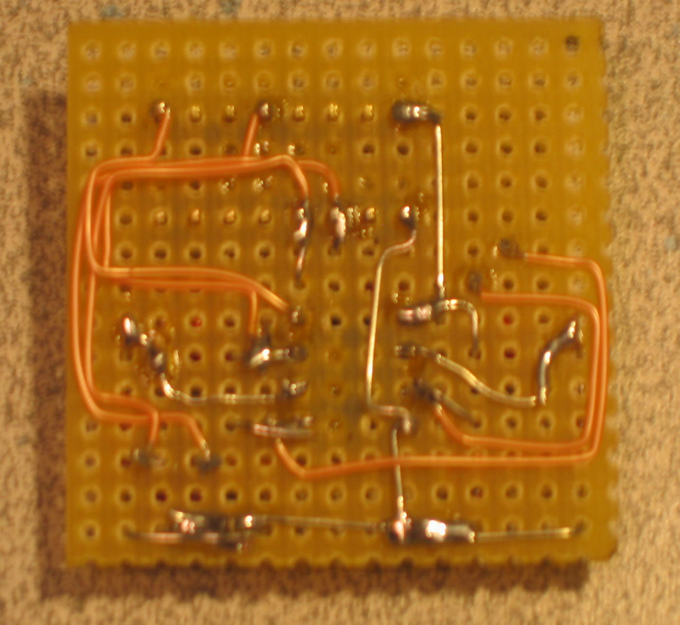
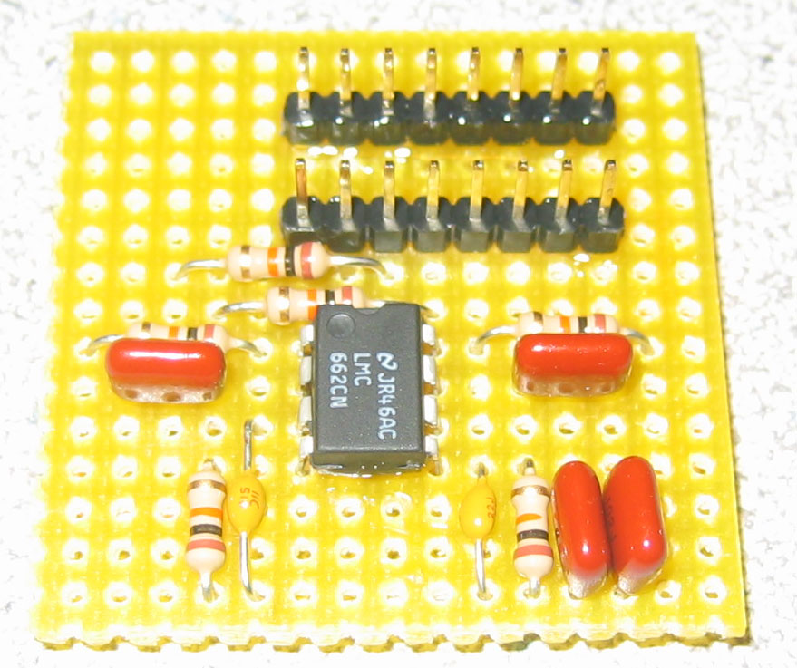
Cut the perf-board to give you 15 holes by 15 holes. Use the photo (click to enlarge) to see the component placement. I used some epoxy to hold the header pins and the IC in place. There isn't any room to mount the IC in a socket, so be careful not to apply too much heat to its pins when soldering.
Use the schematic diagram to connect the components together on the reverse side of the board. Pin 1 of the header assembly is the lower right pin in the picture. Remember that this board will plug in to the main logic board with these components facing downwards.
Figure 1. daughterboard.pdf
Table 2. Parts List
| U1 | LMC662CN |
| R1 | 10K 1/4W 5% |
| R2 | 10K 1/4W 5% |
| R3 | 10K 1/4W 5% |
| R4 | 10K 1/4W 5% |
| R5 | 10K 1/4W 5% |
| R6 | 10K 1/4W 5% |
| R7 | 10K 1/4W 5% |
| R8 | 10K 1/4W 5% |
| C1 | 1.0nF |
| C2 | 22pF |
| C3 | 100pF |
| C4 | 100pF |
| C5 | 1.0nF |
| C6 | 22pF |
| Perf-board (15 holes by 15 holes) | |
| 2 x 8-pin header strip | |
| Epoxy glue |
Re-Assembly
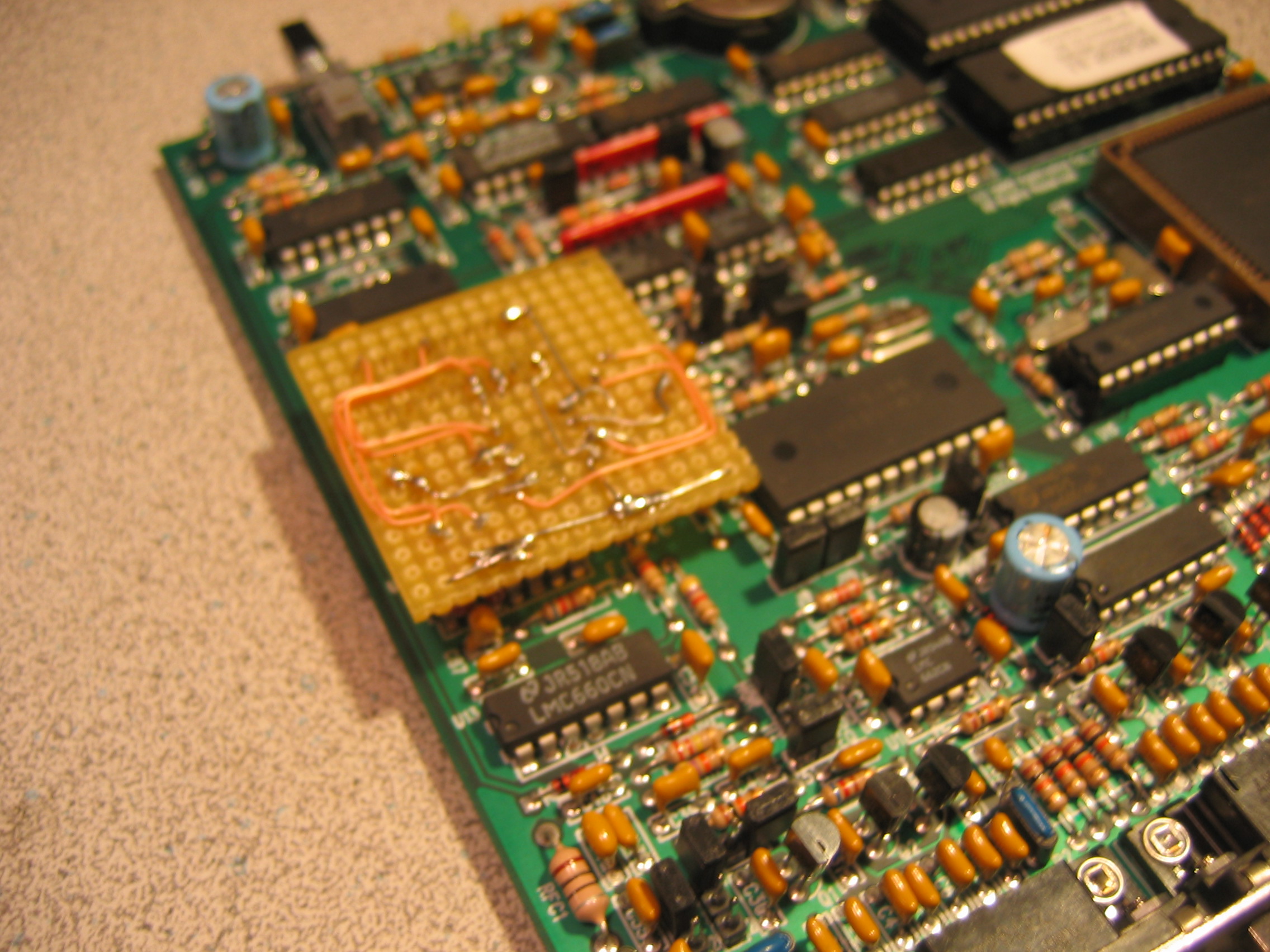 Now it's
time for re-assembly and testing. Start by mounting the main logic board
back inside the case. Once the board is mounted correctly, plug the
daughter card in to the main logic board, paying close attention to the
orientation.
Now it's
time for re-assembly and testing. Start by mounting the main logic board
back inside the case. Once the board is mounted correctly, plug the
daughter card in to the main logic board, paying close attention to the
orientation.
It's important to make sure that the daughter board doesn't work loose once in service. In the prototype, I used a stick-on rubber foot mounted on the top of the daughter board. This foot presses against the top of the case once assembled, and holds the daughter board in place.
Usage
Table 3 shows the appropriate pin-outs for analog inputs on your modified KPC-9612+MX. To monitor a voltage source (such as a battery), use a multi-turn potentiometer between the voltage source and ground, with the wiper connected to an analog input. In the prototype, I adjusted the potentiometer so that a voltage value of 25.5v corresponded to an analog reading of 255.
To measure temperature, set up a voltage divider, with a thermistor between the +5v output and an analog input, and a fixed resistor (or potentiometer) between the analog input and ground. Unfortunately, thermistors do not provide a linear response, so an external application will have to convert the telemetry reading to an actual temperature. Conversion can either be done using a lookup table, or calculating values using the beta value of the thermistor.
Table 3. Pin-Outs
| DB15 pin 14 | Analog 0 |
| DB15 pin 15 | Analog 1 |
| DB25 pin 12 | Analog 2 |
| DB25 pin 13 | Analog 3 |
| DB25 pin 11 | +5v |
| DB25 pin 1 | Ground |
Summary
This modification has successfully been implemented in two mountain-top APRS repeater systems. I hope you find it useful in your application. Feel free to contact me if you have any questions or comments.